Passband modulation
|
See also
|
In electronics and telecommunications, modulation is the process of varying
one or more properties of a periodic waveform, called the carrier
signal,
with a modulating signal which typically contains
information to be transmitted. This is done in a similar fashion to a musician modulating a tone (a periodic
waveform) from a musical instrument by varying its volume, timing and pitch. The three key parameters
of a periodic waveform are its amplitude("volume"), its phase ("timing") and
its frequency ("pitch"). Any of
these properties can be modified in accordance with a low frequency signal to
obtain the modulated signal. Typically a high-frequency sinusoid waveform is used as carrier
signal,
but a square wave pulse train may also be used.
In telecommunications, modulation is the process
of conveying a message signal, for example a digital bit stream or an analog audio signal, inside
another signal that can be physically transmitted. Modulation of a sine
waveform is used to transform a baseband message signal into a passband signal, for example
low-frequency audio signal into a radio-frequency signal (RF signal). In radio
communications, cable TV systems or the public switched telephone
network for instance, electrical signals can only be
transferred over a limited passband frequency spectrum, with specific
(non-zero) lower and upper cutoff frequencies. Modulating a sine-wave carrier
makes it possible to keep the frequency content of the transferred signal as
close as possible to the centre frequency (typically the carrier frequency) of
the passband.
A device that performs modulation is known as
a modulator and a device that performs the inverse operation of modulation is
known as a demodulator(sometimes detector or demod). A device that can do
both operations is a modem (from "modulator–demodulator").
The aim of digital modulation is to transfer a digital bit stream over an analog bandpass channel, for example over the public switched telephone
network (where a bandpass filter limits the frequency range
to between 300 and 3400 Hz), or over a limited radio frequency band.
The aim of analog modulation is to transfer an analog baseband (or lowpass) signal, for
example an audio signal or TV signal, over an analog bandpass channel at a different frequency,
for example over a limited radio frequency band or a cable TV network channel.
Analog and digital modulation facilitate frequency division
multiplexing (FDM), where several low pass information
signals are transferred simultaneously over the same shared physical medium,
using separate passband channels (several different carrier frequencies).
The aim of digital baseband modulation methods, also known as line
coding,
is to transfer a digital bit stream over a baseband channel, typically a
non-filtered copper wire such as a serial
busor
a wired local area network.
The aim of pulse modulation methods is to transfer a narrowband analog signal, for example
a phone call over a wideband baseband channel or, in
some of the schemes, as a bit stream over another digital transmission system.
In music synthesizers, modulation may be used
to synthesise waveforms with an extensive overtone spectrum using a small
number of oscillators. In this case the carrier frequency is typically in the
same order or much lower than the modulating waveform. See for example frequency modulation
synthesis or ring modulation synthesis.
Contents
|

A low-frequency message
signal (top) may be carried by an AM or FM radio wave.
In analog modulation, the modulation
is applied continuously in response to the analog information signal. Common
analog modulation techniques are:[1]
·
Amplitude modulation (AM) (here the amplitude of
the carrier signal is varied in accordance to the instantaneous amplitude of
the modulating signal)
·
Double-sideband
modulation (DSB)
·
Double-sideband
modulation with carrier (DSB-WC) (used on the AM radio broadcasting band)
·
SSB
with carrier (SSB-WC)
·
SSB
suppressed carrier modulation (SSB-SC)
·
Frequency modulation (FM) (here the frequency of
the carrier signal is varied in accordance to the instantaneous amplitude of
the modulating signal)
·
Phase
modulation (PM) (here the phase shift of the carrier
signal is varied in accordance to the instantaneous amplitude of the modulating
signal)
In digital modulation, an analog
carrier signal is modulated by a discrete signal. Digital modulation methods
can be considered as digital-to-analog conversion, and the corresponding demodulationor
detection as analog-to-digital conversion. The changes in the carrier signal
are chosen from a finite number of M alternative symbols (the modulation alphabet).

Schematic of 4 baud (8
bit/s) data link containing arbitraily chosen values.
A
simple example: A telephone line is designed for transferring
audible sounds, for example tones, and not digital bits (zeros and ones).
Computers may however communicate over a telephone line by means of modems,
which are representing the digital bits by tones, called symbols. If there are
four alternative symbols (corresponding to a musical instrument that can
generate four different tones, one at a time), the first symbol may represent
the bit sequence 00, the second 01, the third 10 and the fourth 11. If the
modem plays a melody consisting of 1000 tones per second, the symbol
rate is 1000 symbols/second, or baud. Since each tone (i.e.,
symbol) represents a message consisting of two digital bits in this example,
the bit
rate is twice the symbol rate, i.e. 2000 bits per
second. This is similar to the technique used by dialup modems as opposed to DSLmodems.
According to one definition of digital
signal,
the modulated signal is a digital
signal,
and according to another definition, the modulation is a form of digital-to-analog conversion. Most textbooks would
consider digital modulation schemes as a form of digital transmission, synonymous to data
transmission;
very few would consider it as analog transmission.
·
QAM (quadrature amplitude
modulation): a
finite number of at least two phases and at least two amplitudes are used.
In QAM, an inphase signal (the I signal, for
example a cosine waveform) and a quadrature phase signal (the Q signal, for
example a sine wave) are amplitude modulated with a finite number of
amplitudes, and summed. It can be seen as a two-channel system, each channel
using ASK. The resulting signal is equivalent to a combination of PSK and ASK.
In all of the above methods, each of these
phases, frequencies or amplitudes are assigned a unique pattern of binary bits. Usually, each phase,
frequency or amplitude encodes an equal number of bits. This number of bits
comprises the symbol that is represented by the
particular phase, frequency or amplitude.
If the alphabet consists of  alternative symbols, each
symbol represents a message consisting of N bits. If the symbol
rate (also known as the baud rate) is
alternative symbols, each
symbol represents a message consisting of N bits. If the symbol
rate (also known as the baud rate) is  symbols/second (orbaud), the data rate is
  bit/second.
For example, with an alphabet consisting of
16 alternative symbols, each symbol represents 4 bits. Thus, the data rate is
four times the baud rate.
In the case of PSK, ASK or QAM, where the
carrier frequency of the modulated signal is constant, the modulation alphabet
is often conveniently represented on a constellation diagram, showing the amplitude of
the I signal at the x-axis, and the amplitude of the Q signal at the y-axis,
for each symbol.
PSK and ASK, and sometimes also FSK, are
often generated and detected using the principle of QAM. The I and Q signals
can be combined into a complex-valued signal I+jQ (where j is theimaginary
unit).
The resulting so called equivalent lowpass signal or equivalent baseband signal is a complex-valued
representation of the real-valued modulated physical signal
(the so-calledpassband signal or RF
signal).
1. Group the incoming data
bits into codewords, one for each symbol that will be transmitted.
2. Map the codewords to
attributes, for example amplitudes of the I and Q signals (the equivalent low
pass signal), or frequency or phase values.
3. Adapt pulse
shaping or some other filtering to limit the
bandwidth and form the spectrum of the equivalent low pass signal, typically
using digital signal processing.
4. Perform digital to analog
conversion (DAC) of the I and Q signals (since today all of the above is
normally achieved using digital signal processing, DSP).
5. Generate a high frequency
sine carrier waveform, and perhaps also a cosine quadrature component. Carry
out the modulation, for example by multiplying the sine and cosine waveform
with the I and Q signals, resulting in the equivalent low pass signal being
frequency shifted to the modulated passband signal or RF
signal.
Sometimes this is achieved using DSP technology, for example direct digital synthesis using a waveform table, instead of analog signal
processing. In that case the above DAC step should be done after this step.
6. Amplification and analog
bandpass filtering to avoid harmonic distortion and periodic spectrum
1. Bandpass filtering.
3. Frequency shifting of the
RF signal to the equivalent baseband I and Q signals, or to an intermediate
frequency (IF) signal, by multiplying the RF signal with a local oscillator
sinewave and cosine wave frequency (see the superheterodyne receiver principle).
4. Sampling and
analog-to-digital conversion (ADC) (Sometimes before or instead of the above
point, for example by means of undersampling).
5. Equalization filtering, for
example a matched
filter,
compensation for multipath propagation, time spreading, phase distortion and
frequency selective fading, to avoid intersymbol interferenceand symbol distortion.
6. Detection of the amplitudes
of the I and Q signals, or the frequency or phase of the IF signal.
7. Quantization of the
amplitudes, frequencies or phases to the nearest allowed symbol values.
8. Mapping of the quantized
amplitudes, frequencies or phases to codewords (bit groups).
9. Parallel-to-serial
conversion of the codewords into a bit stream.
10. Pass the resultant bit
stream on for further processing such as removal of any error-correcting codes.
As is common to all digital communication
systems, the design of both the modulator and demodulator must be done
simultaneously. Digital modulation schemes are possible because the
transmitter-receiver pair have prior knowledge of how data is encoded and
represented in the communications system. In all digital communication systems,
both the modulator at the transmitter and the demodulator at the receiver are
structured so that they perform inverse operations.
Non-coherent modulation methods do not require a
receiver reference clock signal that is phase synchronized with the sender carrier
wave.
In this case, modulation symbols (rather than bits, characters, or data
packets) are asynchronously transferred. The opposite
is coherent modulation.
The most common digital modulation techniques
are:
·
Binary
PSK (BPSK), using M=2 symbols
·
Quadrature
PSK (QPSK), using M=4 symbols
·
8PSK,
using M=8 symbols
·
16PSK,
using M=16 symbols
·
Differential
PSK (DPSK)
·
Differential
QPSK (DQPSK)
·
π/4–QPSK
MSK and GMSK are particular cases of
continuous phase modulation. Indeed, MSK is a particular case of the sub-family
of CPM known as continuous-phase
frequency-shift keying (CPFSK) which is defined by a rectangular
frequency pulse (i.e. a linearly increasing phase pulse) of one symbol-time
duration (total response signaling).
OFDM is based on the idea of frequency-division
multiplexing (FDM), but the multiplexed streams are all
parts of a single original stream. The bit stream is split into several
parallel data streams, each transferred over its own sub-carrier using some
conventional digital modulation scheme. The modulated sub-carriers are summed
to form an OFDM signal. This dividing and recombining helps with handling
channel impairments. OFDM is considered as a modulation technique rather than a
multiplex technique, since it transfers one bit stream over one communication
channel using one sequence of so-called OFDM symbols. OFDM can be extended to
multi-user channel access method in the orthogonal
frequency-division multiple access (OFDMA) and multi-carrier code
division multiple access (MC-CDMA) schemes, allowing several users to
share the same physical medium by giving different sub-carriers or spreading codes to different users.
Of the two kinds of RF power amplifier, switching amplifiers (Class
D amplifiers)
cost less and use less battery power than linear
amplifiers of the same output power. However, they only
work with relatively constant-amplitude-modulation signals such as angle
modulation (FSK or PSK) and CDMA, but not with QAM and OFDM. Nevertheless,
even though switching amplifiers are completely unsuitable for normal QAM
constellations, often the QAM modulation principle are used to drive switching
amplifiers with these FM and other waveforms, and sometimes QAM demodulators
are used to receive the signals put out by these switching amplifiers.
Automatic digital modulation recognition in
intelligent communication systems is one of the most important issues in software defined radio and cognitive
radio.
According to incremental expanse of intelligent receivers, automatic modulation
recognition becomes a challenging topic in telecommunication systems and computer
engineering. Such systems have many civil and military applications. Moreover,
blind recognition of modulation type is an important problem in commercial
systems, especially in software defined radio. Usually in such systems,
there are some extra information for system configuration, but considering
blind approaches in intelligent receivers, we can reduce information overload
and increase transmission performance.[2] Obviously, with no
knowledge of the transmitted data and many unknown parameters at the receiver,
such as the signal power, carrier frequency and phase offsets, timing information,
etc., blind identification of the modulation is a difficult task. This becomes
even more challenging in real-world scenarios with multipath fading,
frequency-selective and time-varying channels.[3]
There are two main approaches to automatic
modulation recognition. The first approach uses likelihood-based methods to
assign an input signal to a proper class. Another recent approach is based on
feature extraction.
The term digital baseband modulation (or digital baseband
transmission) is synonymous to line
codes.
These are methods to transfer a digital bit stream over an analog baseband channel (a.k.a. lowpass channel) using a pulse
train, i.e. a discrete number of signal levels, by directly modulating the
voltage or current on a cable. Common examples are unipolar, non-return-to-zero(NRZ), Manchester and alternate mark inversion (AMI) codings.[4]
|
Pulse modulation schemes aim at transferring
a narrowband analog signal over an analog baseband channel as a two-level signal
by modulating a pulse
wave.
Some pulse modulation schemes also allow the narrowband analog signal to be
transferred as a digital signal (i.e. as a quantized discrete-time signal) with a fixed bit rate,
which can be transferred over an underlying digital transmission system, for
example some line
code.
These are not modulation schemes in the conventional sense since they are not channel
coding schemes, but should be considered as source
coding schemes, and in some cases analog-to-digital
conversion techniques.
Analog-over-analog methods:
Analog-over-digital methods:
TCP/ip and osi model:
OSI
Model (7 layers)
|
Internet
Model (4 layers)
|
|||
Layer
Name
|
Layer
Name
|
Protocol
|
Address
|
|
Application
|
Application
|
Telnet, SSH
|
hostname
|
|
Presentation
|
E-mail
|
user@domain
|
||
Session
|
Web Browser
|
URL
|
||
Transport
|
Transport
|
Transmission Control
Protocol
or User Datagram Protocol |
Port Numbers
|
|
Network
|
Network
|
Interrnet Protocol
|
IP Address
|
|
Data
Link
|
Network
Interface |
Network Interface
Device
FastEthernet, GigE, WiFi (802.11a, b, g, n) |
MAC Address
|
|
Physical
|
||||
OSI 7 LAYERS:
The
OSI, or Open System Interconnection, model defines a networking framework to
implement protocols in seven layers. This article explains the 7 Layers of the
OSI Model.
The OSI, or Open System Interconnection, model defines a
networking framework to implement protocols in seven layers. Control is passed
from one layer to the next, starting at the application layer in one station,
and proceeding to the bottom layer, over the channel to the next station and
back up the hierarchy.
Application
(Layer 7)
This
layer supports application and end-user processes.
Communication partners are identified, quality of service is identified, user
authentication and privacy are considered, and any constraints on data syntax are identified. Everything
at this layer is application-specific. This layer provides application services
for file transfers, e-mail, and other network software services. Telnet and FTP are applications that
exist entirely in the application level. Tiered application architectures are
part of this layer.
Presentation
(Layer 6)
Sponsored
This
layer provides independence from differences in data representation (e.g., encryption) by translating from
application to network format, and vice versa. The presentation layer works to
transform data into the form that the application layer can accept. This layer
formats and encrypts data to be sent across a network, providing freedom from
compatibility problems. It is sometimes called the syntax layer.
Session
(Layer 5)
This
layer establishes, manages and terminates connections between applications. The session layer sets
up, coordinates, and terminates conversations, exchanges, and dialogues between
the applications at each end. It deals with session and connection
coordination.
Transport
(Layer 4)
This
layer provides transparent transfer of data between end systems, or hosts, and is responsible for
end-to-end error recovery and flow control. It ensures complete
data transfer.
Network
(Layer 3)
This
layer provides switching and routing technologies, creating
logical paths, known as virtual circuits, for transmitting data
from node to node. Routing and
forwarding are functions of this layer, as well as addressing, internetworking, error handling,congestion control and packet sequencing.
Data
Link (Layer 2)
At
this layer, data packets are encoded and decoded into bits. It
furnishes transmission protocol knowledge and management
and handles errors in the physical layer, flow control and frame
synchronization. The data link layer is divided into two sub layers: The Media
Access Control (MAC) layer and the Logical Link Control (LLC) layer. The MAC sub
layer controls how a computer on the network gains access to the data and
permission to transmit it. The LLC layer controls framesynchronization, flow control and error
checking.
Physical
(Layer 1)
This
layer conveys the bit stream - electrical impulse, light or radio signal --
through the network at the electrical and
mechanical level. It provides the hardware means of sending and
receiving data on a carrier, including defining cables, cards and physical
aspects. Fast Ethernet, RS232, and ATM are protocols with physical layer components.
The
TCP/IP model
TCP/IP
is based on a four-layer reference model. All protocols that belong to the
TCP/IP protocol suite are located in the top three layers of this model.
As
shown in the following illustration, each layer of the TCP/IP model corresponds
to one or more layers of the seven-layer Open Systems Interconnection (OSI)
reference model proposed by the International Standards Organization (ISO).

The
types of services performed and protocols used at each layer within the TCP/IP
model are described in more detail in the following table.
Layer
|
Description
|
Protocols
|
Application
|
Defines TCP/IP
application protocols and how host programs interface with transport layer
services to use the network.
|
HTTP, Telnet, FTP,
TFTP, SNMP, DNS, SMTP, X Windows, other application protocols
|
Transport
|
Provides communication
session management between host computers. Defines the level of service and
status of the connection used when transporting data.
|
TCP, UDP, RTP
|
Internet
|
Packages data into IP
datagrams, which contain source and destination address information that is
used to forward the datagrams between hosts and across networks. Performs
routing of IP datagrams.
|
IP, ICMP, ARP, RARP
|
Network interface
|
Specifies details of
how data is physically sent through the network, including how bits are
electrically signaled by hardware devices that interface directly with a
network medium, such as coaxial cable, optical fiber, or twisted-pair copper
wire.
|
Ethernet, Token Ring,
FDDI, X.25, Frame Relay, RS-232, v.35
|
====================================================
Multiplexer
Description
This component contains a
multiplexer for boolean values. The multiplexer routes one of the input values
to the output connector. The selected input connector depends on the address
read from the address inputs.
The component has an internal
address latch. This latch is activated if the optional connector 'Enable Latch
Address' is activated. During true condition at this input the current address
is used. A change to false condition latches the address. During false
condition at this input the latched address is used. The latch is bypassed if
the optional connector 'Enable Latch Address' is deactivated.
The component also has an
internal output latch. This latch is activated if the connector 'Enable Latch
Output' is activated. During true condition at this input the current addressed
input value is used. A change to false condition latches the output value.
During false condition at this input the latched output value is used. The
latch is bypassed if the optional connector 'Enable Latch Output' is
deactivated.
If an input is addressed which
does not exist (e.g. the 15th input is selected but the component has only 14
inputs) the reset value is used.
Features
·
Up to 16 inputs.
·
The all inputs and outputs are negatable.
·
The 'Latch Address Input' and 'Latch Output' inputs are level or
edge sensitive.
·
Activate or deactivate the optional 'Latch Address Input' and
'Latch Output' inputs (deactivated connectors are hidden).
·
The component is rotatable.
View


Truth Table
Address A
|
Address B
|
Input A
|
Input B
|
Input C
|
Input D
|
Output
|
|
False
|
False
|
False
|
X
|
X
|
X
|
False
|
|
False
|
False
|
True
|
X
|
X
|
X
|
True
|
|
True
|
False
|
X
|
False
|
X
|
X
|
False
|
|
True
|
False
|
X
|
True
|
X
|
X
|
True
|
|
False
|
True
|
X
|
X
|
False
|
X
|
False
|
|
False
|
True
|
X
|
X
|
True
|
X
|
True
|
|
True
|
True
|
X
|
X
|
X
|
False
|
False
|
|
True
|
True
|
X
|
X
|
X
|
True
|
True
|
The truth table shows a 4-input multiplexer.
Enable Output Latch
|
Address A
|
Input A
|
Input B
|
Output(t)
|
|
True
|
False
|
False
|
X
|
False
|
|
True
|
False
|
True
|
X
|
True
|
|
True
|
True
|
X
|
False
|
False
|
|
True
|
True
|
X
|
True
|
True
|
|
False
|
X
|
X
|
X
|
Output(t-1)
|
The truth table shows a 2-input multiplexer width
output latch. The enable input of the output latch input is level senitive.
Location
Boolean -> Mux & Demux
-> Multiplexer
Demultiplexer
Description
This component contains a
demultiplexer for boolean values. The demultiplexer routes the input value to
one of the output connectors. The selected output connector depends on the
address read from the address inputs.
The component has an internal
address latch. This latch is activated if the optional connector 'Enable Latch
Address' is activated. During true condition at this input the current address
is used. A change to false condition latches the address. During false
condition at this input the latched address is used. The latch is bypassed if
the optional connector 'Enable Latch Address' is deactivated.
The component also has an
internal output latch. This latch is activated if the connector 'Enable Latch
Output' is activated. During true condition at this input the latch is
bypassed. A change to false condition latches the last output values. During
false condition at this input the latched output values are used. The latch is
bypassed if the optional connector 'Enable Latch' is deactivated.
Features
·
Up to 16 outputs.
·
The all inputs and outputs are negatable.
·
The 'Latch Address Input' input are level or edge sensitive.
·
Activate or deactivate the optional 'Latch Address Input'
(deactivated connectors are hidden).
·
The component is rotatable.
View


Truth Table
Address A
|
Address B
|
Input
|
Output A
|
Output B
|
Output C
|
Output D
|
|
X
|
X
|
False
|
False
|
False
|
False
|
False
|
|
False
|
False
|
True
|
True
|
False
|
False
|
False
|
|
True
|
False
|
True
|
False
|
True
|
False
|
False
|
|
False
|
True
|
True
|
False
|
False
|
True
|
False
|
|
True
|
True
|
True
|
False
|
False
|
False
|
True
|
The truth table shows a 4-output demultiplexer
(or a 2-to-4 decoder).
Enable Output Latch
|
Address A
|
Input
|
Output A(t)
|
Output B(t)
|
|
True
|
X
|
False
|
False
|
False
|
|
True
|
False
|
True
|
True
|
False
|
|
True
|
True
|
True
|
False
|
True
|
|
False
|
X
|
X
|
Output A(t-1)
|
Output B(t-1)
|
The truth table shows a 2-input multiplexer width
output latch. The enable input of the output latch input is level senitive.
Location
Boolean
-> Mux & Demux -> Demultiplexe
Digital Electronics: Types of Flip-Flop Circuits?
In electronics, a flip-flop is a special type of gated latch circuit.
There are several different types of flip-flops. The most common types of flip
flops are:
·
SR flip-flop: Is similar to an SR latch. Besides the
CLOCK input, an SR flip-flop has two inputs, labeled SET and RESET. If the SET
input is HIGH when the clock is triggered, the Q output goes HIGH. If the RESET
input is HIGH when the clock is triggered, the Q output goes LOW.
Note
that in an SR flip-flop, the SET and RESET inputs shouldn't both be HIGH when
the clock is triggered. This is considered an invalid input condition, and the
resulting output isn't predictable if this condition occurs.
·
D flip-flop: Has just one input in addition to the CLOCK
input. This input is called the DATA input. When the clock is triggered, the Q
output is matched to the DATA input. Thus, if the DATA input is HIGH, the Q
output goes HIGH, and if the DATA input is LOW, the Q output goes LOW.
Most
D-type flip-flops also include S and R inputs that let you set or reset the
flip-flop. Note that the S and R inputs in a D flip-flop ignore the CLOCK
input. Thus, if you apply a HIGH to either S or R, the flip-flop will be set or
reset immediately, without waiting for a clock pulse.
·
JK flip-flop: A common variation of the SR flip-flop. A
JK flip-flop has two inputs, labeled J and K.The J input corresponds to the
SET input in an SR flip-flop, and the K input corresponds to the RESET input.
The
difference between a JK flip-flop and an SR flip-flop is that in a JK flip-flop,
both inputs can be HIGH. When both the J and K inputs are HIGH, the Q output is toggled, which means that the
output alternates between HIGH and LOW.
For
example, if the Q output is HIGH when the clock is triggered and J and K are
both HIGH, the Q output is set to LOW. If the clock is triggered again while J
and K both remain HIGH, the Q output is set to HIGH again, and so forth, with
the Q output alternating from HIGH to LOW at every clock tick.
·
T flip-flop: This is simply a JK flip-flop whose output
alternates between HIGH and LOW with each clock pulse. Toggles are widely used
in logic circuits because they can be combined to form counting circuits that
count the number of clock pulses received.
You can
create a T flip-flop from a D flip-flop by connecting the Q-bar output directly to the D input. Thus,
whenever a clock pulse is received, the current state of the Q output is inverted (that’s what the Q-bar output is) and fed back into the D input.
This causes the output to alternate between HIGH and LOW.
You can
also create a T flip-flop from a JK flip-flop simply by hard-wiring both the J
and K inputs to HIGH. When both J and K are HIGH, the JK flip-flop acts as a
toggle.
Although you can construct your
own flip-flop circuits using NAND gates, it’s much easier to use integrated
circuits (ICs) that contain flip-flops. One common example is the 4013 Dual D
Flip-Flop. This chip contains two D-type flip-flops in a 14-pin DIP package.
Pin
|
Name
|
Explanation
|
Pin
|
Name
|
Explanation
|
1
|
Q1
|
Flip-flop 1 Q output
|
8
|
SET2
|
Flip-flop 2 SET input
|
2
|
Q1-bar
|
Flip-flop 1 Q-bar output
|
9
|
DATA2
|
Flip-flop 2 DATA input
|
3
|
CLOCK1
|
Flip-flop 1 CLOCK input
|
10
|
RESET2
|
Flip-flop 2 RESET input
|
4
|
RESET1
|
Flip-flop 1 RESET input
|
11
|
CLOCK2
|
Flip-flop 2 CLOCK input
|
5
|
DATA1
|
Flip-flop 1 DATA input
|
12
|
Q2-bar
|
Flip-flop 2 Q-bar output
|
6
|
SET
|
Flip-flop 1 SET input
|
13
|
Q2
|
Flip-flop 2 Q output
|
7
|
GND
|
Ground
|
14
|
VDD
|
+3 to 15 V
|
Synchronous
and Asynchronous Counters in Digital Electronics
A counter is a sequential circuit that
counts in a cyclic sequence. It is essentially a register that goes
through a predetermined sequence of states upon the application of input
pulses. There are two types of counters – Synchronous Counter & Asynchronous
Counter.
Synchronous Counter
In a synchronous counter, the input pulses are applied to all
clock pulse inputs of all flip flops simultaneously (directly). Synchronous
counter is also known asparallel
sequential circuit. Examples of Synchronous Counters are as
below:
Asynchronous Counter
In an asynchronous counter, the flip flop output
transition serves as a source for triggering other flip flops. In other words,
the clock pulse inputs of all flip flops, except the first, are triggered not
by the incoming pulses, but rather by the transition that occurs in previous flip flop’s output.. Asynchronous counter is also known
as serial
sequential circuit. Example of Asynchronous Counters are as
below:
Synchronous counters are faster
than asynchronous counter because in synchronous counter all flip flops are
clocked simultaneously.
Ring
Counter in Digital Electronics
Ring counter is a synchronous counter since all
the flip flops are clocked simultaneously. A ring counter is a circular shift register with only
one flip flopbeing set at any particular time, all others
are cleared. The single bit is shifted from one flip flop to the
other to produce the sequence of timing signals.
 It is a
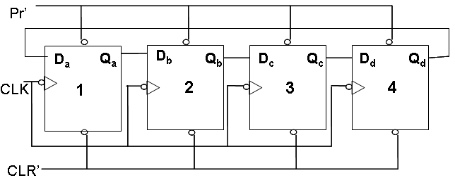
4-bit shift register connected as a ring counter. In this counter, Serial In Da
is connected to Serial Out Qd.
It is a
4-bit shift register connected as a ring counter. In this counter, Serial In Da
is connected to Serial Out Qd.
First of all, CLR’ is set to 0 to clear all flip flops and then
it is set to 1 for the circuit operation. After clearing all the flip flops,
Pr’ of 4th flip flop
is set to 0 while for all other three flip flops, it set to 1. This is done so
that the initial value of register becomes 0001 [Pr’=0, sets the 4th flip flop to 1].
Single bit is shifted right with
every clock pulse. Each flip flop is in 1 state once every four clock pulses.
CLK
|
Qa
|
Qb
|
Qc
|
Qd
|
0
|
0
|
0
|
0
|
0
|
0
|
0
|
0
|
0
|
1
|
1
|
1
|
0
|
0
|
0
|
2
|
0
|
1
|
0
|
0
|
3
|
0
|
0
|
1
|
0
|
4
|
0
|
0
|
0
|
1
|
Disadvantages of Ring Counter
1. Using ring
counter, one can count only four distinct states which is totally wastage of flip
flops.
2. Ring
counter doesn’t count in a binary sequence so it is not preferred.
Mod of the Ring Counter is “n” where n is the number of flip
flops. In a Ring Counter, the frequency of output is divided by n, therefore,
it is known as divide by
N counter.
Johnson
Counter in Digital Electronics
Johnson counter or Switch Tail or Twisted Ring Counter is a synchronous counter. An n-bit ring counter circulates
a single bit among the flip flops to provide n distinct states. The number of
states can be doubled if the shift register is connected as a switch tail ring
counter.
A switch tail ring counter is a circular shift register with the
complement output of the last flip flop connected
to the input of the fist flip flop. The circular connection is made from the
complement output of the rightmost flip flop to the input of the leftmost flip
flop. The register shifts its contents once to the right with every clock pulse
and at the same time, the complement value of flip flop 4 are transferred to flip
flop 1.
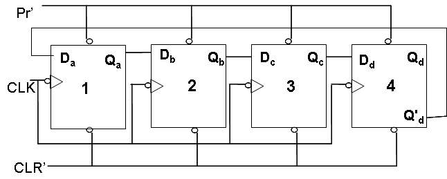 Starting
from cleared states, the 4-bit switch tail ring counter goes through a sequence
of 8 states. In general, a k-bit switch tail ring counter will go through a
sequence of 2k states.
Starting
from cleared states, the 4-bit switch tail ring counter goes through a sequence
of 8 states. In general, a k-bit switch tail ring counter will go through a
sequence of 2k states.
Starting from all 0’s, each shift
operation inserts 1’s from the left until the register is filled with all 1’s.
In the following sequence 0’s are inserted from the left until the register is
again filled with all 0’s.
CLK
|
Qa
|
Qb
|
Qc
|
Qd
|
Qd’
|
0
|
0
|
0
|
0
|
0
|
1
|
1
|
1
|
0
|
0
|
0
|
|
2
|
1
|
1
|
0
|
0
|
|
3
|
1
|
1
|
1
|
0
|
|
4
|
1
|
1
|
1
|
1
|
0
|
5
|
0
|
1
|
1
|
1
|
|
6
|
0
|
0
|
1
|
1
|
|
7
|
0
|
0
|
0
|
1
|
|
8
|
0
|
0
|
0
|
0
|
1
|
Mod of Johnson Counter is 2n,
therefore it is known as Divide by 2N Counter.
Frequency of Output = frequency of
Clock Pulse / mod
fjohnson = f / 2n
Disadvantage of Johnson Counter
Disadvantage of Johnson Counter is
that it doesn’t count in a binary sequence.
Johnson counters can be
constructed for any number of timing sequences. The number of flip flops needed
is one half the numbers of timing signals.
Binary
Ripple Counter in Digital Electronics
A counter that follows the binary sequence is called a binary counter. A binary ripple
counter consists of a series of complementing flip flops (T or JK FF) with the
output of each flip flop connected
to the clock pulse input of the next higher order flip flop. The flip flop holding the least significant
bit receives the incoming count pulses.
It is known as ripple
counter because
the flip flops change one at a time in rapid succession and the signal
propagates through the counter in a ripple fashion. CLK is coming for
subsequent flip flops from previous flip flops and change state only when transition
of previous flip flop’s output is from high to low i.e. from 1 to 0.
 The lowest
order bit Q0 gets complimented with each count pulse. Every time Q0 goes from 1
to 0, it complements Q1. Every time Q1 goes from 1 to 0, it complements Q2 and
so on.
The lowest
order bit Q0 gets complimented with each count pulse. Every time Q0 goes from 1
to 0, it complements Q1. Every time Q1 goes from 1 to 0, it complements Q2 and
so on.
A complimentary
flip flop can be
obtained in 3 ways as described below:
1. Using T
Flip Flop
2. Using JK
Flip Flop with J & K inputs tied together
3. Using D
Flip Flop with the complement output connected to the D input. In this way the
D input is always the complement of the present state and next clock pulse will
cause the flip flop to complement.
CLK
|
Q3
|
Q2
|
Q1
|
Q0
|
0
|
0
|
0
|
0
|
0
|
1
|
0
|
0
|
0
|
1
|
2
|
0
|
0
|
1
|
0
|
3
|
0
|
0
|
1
|
1
|
4
|
0
|
1
|
0
|
0
|
5
|
0
|
1
|
0
|
1
|
6
|
0
|
1
|
1
|
0
|
7
|
0
|
1
|
1
|
1
|
8
|
1
|
0
|
0
|
0
|
9
|
1
|
0
|
0
|
1
|
10
|
1
|
0
|
1
|
0
|
11
|
1
|
0
|
1
|
1
|
12
|
1
|
1
|
0
|
0
|
13
|
1
|
1
|
0
|
1
|
14
|
1
|
1
|
1
|
0
|
15
|
1
|
1
|
1
|
1
|
Mod of Binary Ripple Counter = 2n,, where n
is the number of flip flops
The counter counts in a binary sequence from 0 to 2n-1
Disadvantage of Binary Ripple Counter
This counter is slow as delay of
each flip flop has to be taken into account as they are not clocked
simultaneously.
Up Down
Counter in Digital Electronics
A counter which can be made to
count in either the forward or reverse direction is called an up-down, a
reversible or forward-backward counter.
Down Counter
A binary counter with a reverse
count is called a binary down counter. In a down counter, the binary counter is
decremented by 1 with every input count pulse. The count of a 4-bit down
counter starts from binary 15 and continues to binary counts 14, 13, 12… 0 and
then back to 15. In a binary down counter, outputs are taken from the
complement terminals Q’ of all flip flops.
For a down counter, when Q goes from 0 to 1, Q’ will go from 1
to 0 and complement the next flip flop.
Up Counter
A binary counter with a normal
count is called a binary up counter. In a up counter, the binary counter is
incremented by 1 with every input clock pulse. Outputs are taken drom the
normal output terminal Q of all flip flops. For a up counter when Q goes from 1
to 0, it complements the next flip flop.
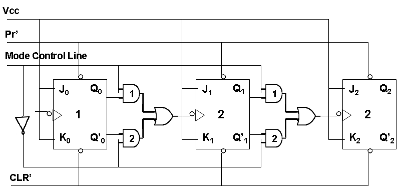
In above diagram, mode
control line is also called up down counter line.
When mode control line is 1, all gates labeled as 1
will be enabled and all gates labeled as 2 will be disabled. The counter works
like a Up
Counter.
When mode control line is 0, all gates labeled as 1
will be disabled and all gates labeles as 1 will be enabled. The counter works
like a Down
Counter.
CLK
|
Q2
|
Q1
|
Q0
|
Q0’
|
Q1’
|
Q2’
|
0
|
0
|
0
|
0
|
1
|
1
|
1
|
1
|
1
|
1
|
1
|
0
|
0
|
0
|
2
|
1
|
1
|
0
|
1
|
0
|
0
|
3
|
1
|
0
|
1
|
0
|
1
|
0
|
4
|
1
|
0
|
0
|
1
|
1
|
0
|
5
|
0
|
1
|
1
|
0
|
0
|
1
|
6
|
0
|
1
|
0
|
1
|
0
|
1
|
7
|
0
|
0
|
1
|
0
|
1
|
1
|
8
|
0
|
0
|
0
|
1
|
1
|
1
|
Shift
Registers In Digital Electronics
There are couple of ways to define
a Register used in Digital Electronics.
“Registers are data storage
devices that are more sophisticated than latches.”
“A register is a group of binary
cells suitable for holding binary information.”
“A group of cascaded flip flops
used to store related bits of information is known as a register.”
Application of Registers
These are used in computers for
·
Temporary storage
·
Data transferring
·
Data manipulation
·
As counters
Shift Register
A register that is used to assemble and store information
arriving from a serial source is called a shift register. Each flip flop output of
a shift register is a connected to the input of the following flip flop and a
common clock pulse is applied to all flip flops, clocking them synchronously.
Hence the shift register is asynchronous sequential circuit. An n-bit shift register consists of n
Flip Flops and the gates control the shift operation.
There are four types of Shift
Registers:
1. Serial-In,
Serial-Out (SISO)
2. Parallel-In,
Serial-Out (PISO)
3. Serial-In,
Parallel-Out (SIPO)
4. Parallel-In,
Parallel-Out (PIPO)
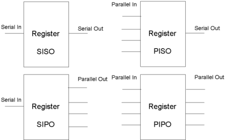
Serial-In, Serial-Out (SISO)
Serial-In, Serial-Out shift register can be constructed by using D flip flops. This type of shift register accepts data
serially i.e. one bit at a time and produces stored information on its output
serially.
Here, four flip flops are
cascaded. Since each flip flop can store only one bit, the register can store
maximum four bits. More flip flops can be cascaded to store more than 4 bits.
Clock is applied simultaneously to all flip flops clocking them synchronously.
We know that in a D Flip Flop, the
Q output is identical to the D input except with one pulse time delay.
Therefore, there will be a delay i.e. it will take one clock pulse to transfer
the bit to next flip flop.
Let’s understand Shifting by
taking an example. Let say the 4-bits applied to serial input are 1010. Here
LSB 0 is applied first and MSB 1 is applied last since the input is applied in
serial fashion.
Now, refer the table below. At
first clock pulse, i.e. when CLK = 1, LSB 0 is applied to Serial In.
At CLK = 2, next bit i.e. 1 is
applied to Serial In. At this moment, 0 applied at CLK=1, shifts to Qa.
At CLK = 3, next bit i.e. 0 is
applied to Serial In. At this moment , 1 applied at CLK = 2 shifts to Qa and o
applied at CLK = 1 shifts to Qb.
And so on. For shifting out, 0′s
are applied at Serial In.
CLK
|
Da / Serial In
|
Qa
|
Qb
|
Qc
|
Qd / Serial Out
|
0
|
0
|
0
|
0
|
0
|
0
|
1
|
0
|
0
|
0
|
0
|
0
|
2
|
1
|
0
|
0
|
0
|
0
|
3
|
0
|
1
|
0
|
0
|
0
|
4
|
1
|
0
|
1
|
0
|
0
|
5
|
0
|
1
|
0
|
1
|
0
|
6
|
0
|
0
|
1
|
0
|
1
|
7
|
0
|
0
|
0
|
1
|
0
|
8
|
0
|
0
|
0
|
0
|
1
|
9
|
0
|
0
|
0
|
0
|
0
|
It will require 4 clock pulses for
Shifting In the data and 4 clock pulses for Shifting Out the data. Thus, for an
n-bit SISO shift register, 2n clock pulses are required.
Serial-In, Parallel-Out (SIPO)
Serial-In, Parallel-Out shift
register can be constructed by using D flip flops. This type of shift register
accepts data serially i.e. one bit at a time and produces stored information on
its output parallely i.e. all the outputs are available simultaneously.
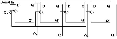
Here, four flip flops are
cascaded. Since each flip flop can store only one bit, the register can store
maximum four bits. More flip flops can be cascaded to store more than 4 bits.
Clock is applied simultaneously to all flip flops clocking them synchronously.
We know that in a D Flip Flop, the
Q output is identical to the D input except with one pulse time delay.
Therefore, there will be a delay i.e. it will take one clock pulse to transfer
the bit to next flip flop. All the outputs are available simultaneously at Qa,
Qb, Qc and Qd.
Note: Circuit
diagram of SIPO is same as SISO except that outputs are available
simultaneously rather than serially at Serial Out.
Parallel-In, Serial-Out (PISO)
Parallel-In shift register can be
constructed by using D flip flops. This type of shift register accepts data
parallely i.e. all the bits are input simultaneously.

·
Serial In is kept at 0.
·
For shifting in the data parallely i.e. all the bits are fed
simultaneously, LOAD=1. Whatever is available at a3 will be applied to Preset input of
flip flop. Thus, the flip flop is set or reset based on the Preset input and
this is how all the input bits are applied in parallel.
·
After shifting the data in, LOAD=0 and output is obtained from
Serial Out.
The data will be available at the
output after 4 clock pulse.
Parallel-In, Parallel-Out (PIPO)
Parallel-In shift register can be
constructed by using D flip flops. This type of shift register accepts data
parallely i.e. all the bits are input simultaneously and produces stored
information on its output parallely i.e. all the outputs are available
simultaneously.
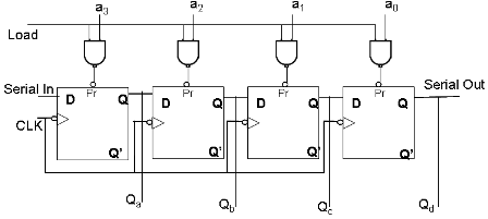
·
Serial In is kept at 0.
·
For shifting in the data parallely i.e. all the bits are fed
simultaneously, LOAD=1. Whatever is available at a3 will be applied to Preset input of
flip flop. Thus, the flip flop is set or reset based on the Preset input and
this is how all the input bits are applied in parallel.
·
After shifting the data in, LOAD=0 and output is obtained from
Parallel Outputs Qa, Qb, Qc and Qd.
No clock pulse is required. Data
can be shifted into or out of the register in parallel.
Note: Circuit
diagram of PIPO is same as PISO except that outputs are available
simultaneously rather than serially at Serial Out.
No comments:
Post a Comment